Developing next-generation spin-polarized electron sources for particle accelerators, in collaboration with ODU ECE and Jefferson Lab.
This work is done in collaboration with the Sylvain Marsillac’s group in Electrical & Computer Engineering, and the Electron Gun Group at Jefferson Lab
Why Spin-Polarized Electrons?
Many important experiments in nuclear and particle physics require electron beams where the electrons all spin in the same direction. At CEBAF at Jefferson Lab in Newport News, Virginia, spin-polarized electrons are used to probe the internal structure of protons and neutrons, map the distribution of quarks and gluons inside the nucleus, and search for signatures of physics beyond the Standard Model. The degree of beam polarization directly determines the sensitivity of these experiments. A more highly polarized beam means cleaner results with less beam time.
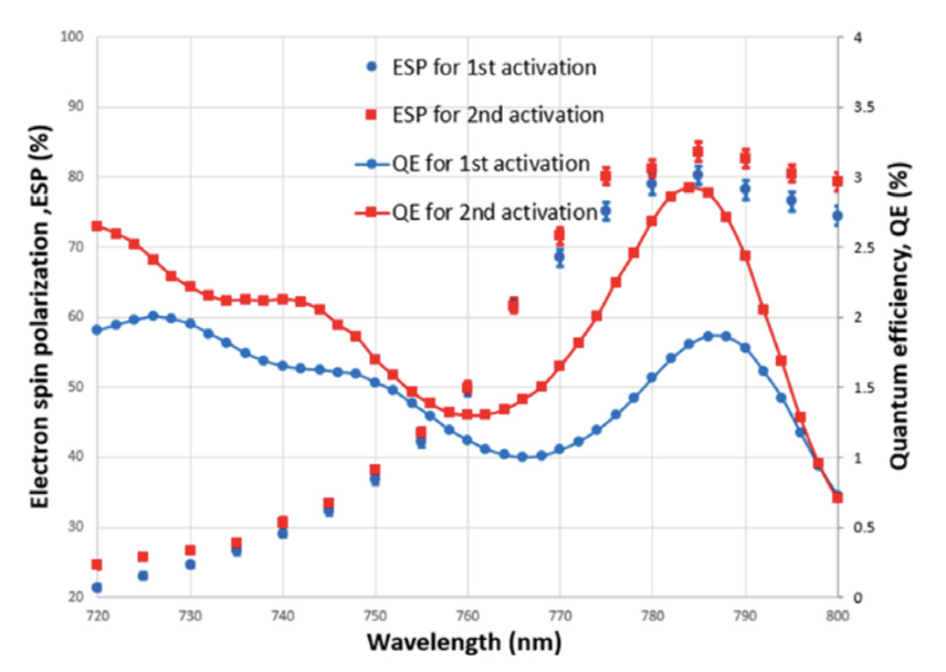
Spin-polarized electron beams are produced by shining a laser on a specially engineered semiconductor called a photocathode, which then emits electrons. The challenge is to make both the spin polarization and the photoemission efficiency (quantum efficiency, or QE) as high as possible simultaneously.
A GaAs-based strained superlattice photocathode mounted on its stalk for installation in the polarized source.
How Strained Semiconductors Produce Spin-Polarized Electrons
In bulk GaAs, the valence band contains two types of states with different total angular momentum: heavy holes ($m_j = \pm 3/2$) and light holes ($m_j = \pm 1/2$). When a circularly polarized laser excites electrons from the valence band to the conduction band, the heavy-hole and light-hole transitions contribute electrons with opposite spin polarization, partially canceling each other out. In a typical crystal, the theoretical maximum polarization is 50%.
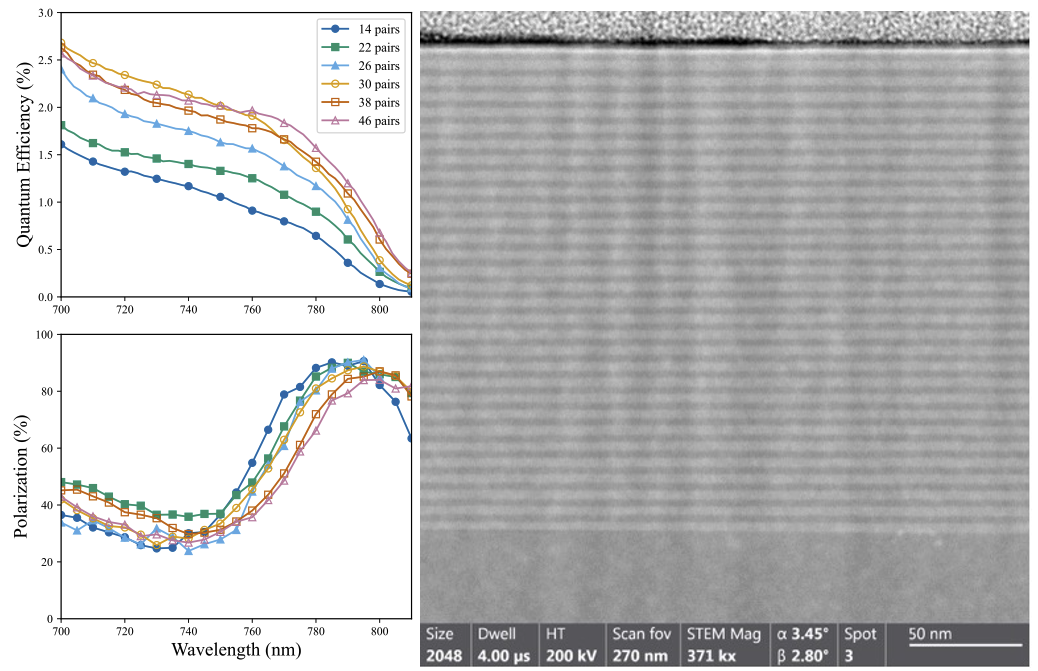
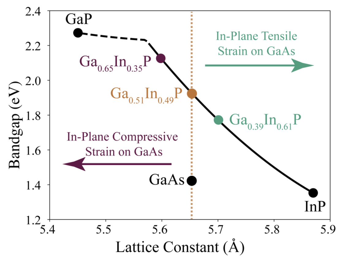
If we apply mechanical strain to the crystal this splits the heavy-hole and light-hole energy bands. If the splitting is large enough, only heavy-hole electrons are excited by the laser, and the photoemitted electrons can reach polarizations approaching 100%. We introduce strain to the photocathode by growing thin layers of GaAs sandwiched between layers of a different semiconductor in a superlattice structure. Mismatched lattice constants between the layers create a built-in compressive or tensile stress that splits the bands.
Schematic band structure of GaAs without strain (left) and with compressive strain (right). Strain splits the heavy-hole (HH) and light-hole (LH) valence bands, enabling selective excitation and spin polarization approaching 100%.
In addition to strain, quantum confinement in the thin GaAs quantum wells further enhances the band splitting. When electrons are confined to a layer only a few nanometers thick, their energies are quantized (like a particle in a box), and the confinement energy shifts the heavy-hole and light-hole levels by different amounts, adding to the strain-induced splitting. By carefully engineering both the composition and thickness of each layer, we can maximize the splitting while maintaining good electron transport to the surface.
Impact of superlattice size on quantum efficiency and polarization in MOCVD-grown strained GaAs/GaAsP photocathodes
Adam Masters, Greg Blume, Sushil Poudel, Joseph Michael Grames, Matt Poelker, Marcy Stutzman, Stephen Polly, Seth M. Hubbard, Sylvain Marsillac, and Matt Grau
Appl. Phys. Lett.128, 8 (Feb 2026)
Strained superlattice GaAs photocathodes are crucial for providing high photocurrent beams of spin-polarized electrons at several accelerator facilities including the Continuous Electron Beam Accelerator Facility at Thomas Jefferson National Accelerator Facility and the future Electron-Ion Collider at Brookhaven National Laboratory. In this work, we study the effects of varying the number of superlattice pairs on the polarization and photocurrent of the photocathodes. We observe a saturation in quantum efficiency beyond 30 pairs, with additional layers yielding minimal photocurrent improvement while noticeably reducing the polarization of the beam.
Modeling strain and quantum confinement in GaAs/Ga$_{x}$In$_{1-x}$P superlattices for spin-polarized electron sources
A. Kachwala, G. Blume, S. Marsillac, J. Grames, and M. Grau
J. Appl. Phys.138, 23 (Dec 2025)
In this study, we systematically design and simulate a series of GaAs-based superlattice configurations aimed at enhancing heavy-hole--light-hole band splitting while simultaneously optimizing band alignment to reduce the conduction band barrier, thereby facilitating efficient electron transport. These combined effects are crucial for achieving high electron spin polarization and high quantum efficiency, the two key performance metrics of next-generation spin-polarized electron sources. We investigated three types of superlattice architectures: (1) compressively strained GaAs wells on GaInP barriers, yielding a maximum band splitting of 140 meV, (2) lattice-matched GaAs/GaInP structures, resulting in the maximum band splitting of 75 meV, and (3) tensile strained GaAs wells on GaInP barriers, with a maximum band splitting of 40 meV. The results demonstrate the tunability of heavy-hole--light-hole band splitting and establish a design framework for high-performance spin-polarized photocathodes based on a combination of strain engineering, quantum confinement, and optimized heterostructure design.
High figure of merit spin polarized electron sources grown via MOCVD
Benjamin Belfore, Adam Masters, Deewakar Poudel, Greg Blume, Stephen Polly, Erdong Wang, Seth M Hubbard, Marcy Stutzman, Joseph Michael Grames, Matt Poelker, Matt Grau, and Sylvain Marsillac
Appl. Phys. Lett.123, 22 (Nov 2023)
Spin polarized photocathodes are key to the future operation of electron accelerators such as the ones at Thomas Jefferson National Accelerator Facility and Brookhaven National Laboratory. Currently, these photocathodes come in short supply due to limited production by molecular beam epitaxy. By developing a process to implement similar structures using metal organic chemical vapor deposition, the availability of these devices can be increased. In this paper, we detail the implementation of recent photocathode advancements via metal organic chemical vapor deposition process and show an improvement in both polarization and quantum efficiency of our devices compared to those fabricated via molecular beam epitaxy, with devices reaching 82\% polarization and 2.9\% quantum efficiency.